One of the major driving forces behind how electronics and other hardware function is the printed circuit board (PCB). This fact is something everyone interested in electronics knows. But for software designers and other non-technical people, a PCB is basically a connector or bridge that supports electrical connections within a device. Therefore, before taking advantage of the benefits they offer, you must first understand PCBs.
In tech-speak, a printed circuit board is a board that mechanically support and electronically connects electronic components in devices. It accomplishes this task through the use of conductive tracks, pads, and other features. These features are usually etched on sheet layers of copper and laminated onto layers of a nonconductive substrate. The components of a PCB are generally or always fastened to the board by soldering.
Using simpler language, the PCB is a board made from plastic which has been reinforced with glass. And attached to the board are copper lines and pads that allow an electrical charge to pass through the PCB to the components of a device. If you have ever opened a calculator or game controller out of curiosity as a kid, you have seen a PCB.
Properties and Characteristics of a PCB
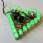
A PCB has distinct characters and components that must be understood before designing or using one. Starting with the conductive tracks, which are also known as circuit traces, the tracks serve as wires. But in this case, they are firmly kept in place and are separated or insulated by air and the substrate material of the board. The conductive tracks have been highlighted in the image below.
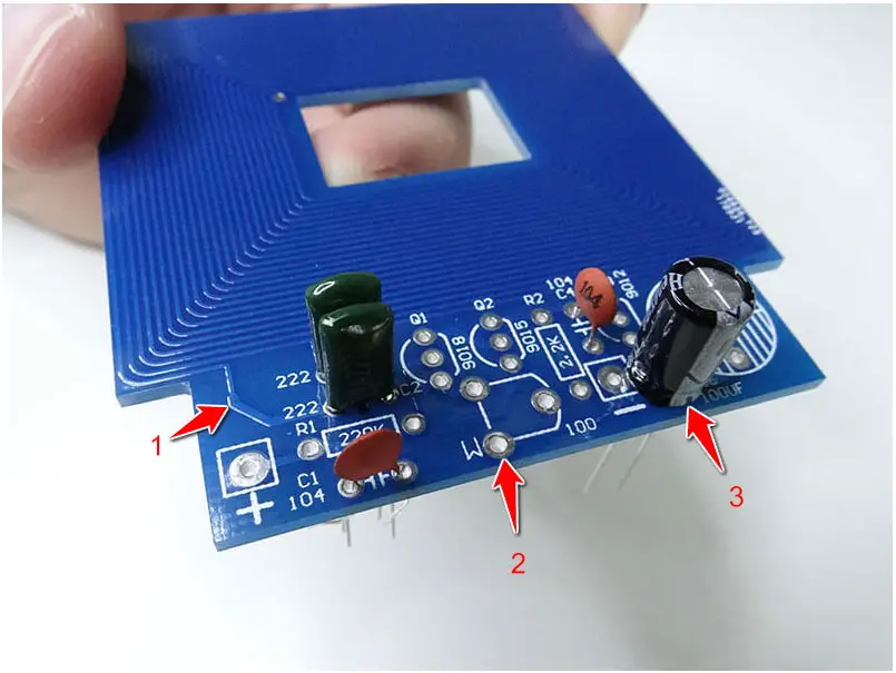
- Conductive tracks
- through-holes
- Components
A PCB is also designed with pads and this serves as connectors, while vias pass the connection between the board’s layers of copper and other solid conductive features on the board. Depending on what a board is built to achieve, other conductors, and components are usually mounted on the board. A PCB can be designed to have multiple copper layers according to how they will be applied. For example, a two-layer has copper layers on both sides of the board. A multi-layered board integrates even more copper layers between the layers of its insulating material.
The components on a PCB are mounted on it through two popular methods. The first is method involves through-holes. Here, components with wire leads are passed through the board and are soldered to traces on the other end. This mechanically keeps the component in place and connects it electronically through the traces. The second mounting technique is the surface-mount. Here, the component lead is soldered to traces on the same surface as the component.
Both mounting methods are generally used interchangeably on a circuit board. The old rule of thumb, which is still efficient, is heavier components like capacitors should be secured using a through-hole and lighter components using a surface-hole. Lastly, the pattern to be etched on the copper layers is called artworks. Artworks are designed using photoresist and are etched firmly by light exposure. Now you know the basics and different components of the board, understanding the design process is the next phase.
The Techniques for Designing a PCB Board
There are a couple of ways to go about designing a PCB board. The three commonly used methods are:
- Iron on glossy paper
- Circuit by hand on PCB
- Laser cutting edge etching method.
With these three methods, the basic design process still remains the same. The design process is started by drafting the schematics for your board using CAD software or PCB layout software. Currently, you can find many open-source applications such as PCB Wizard to help you with this task. The next step is cutting the copper board and transferring the PCB print onto the copper layer. To make this process more relatable below is a highlight or outline of the steps:
- Design Schematics – With the aid of CAD software, you can easily design your own schematics or borrow one from the public library of the app you chose.
- Take a Printout of Your Circuit Board Layout – The print out should be taken using an A4 photo paper. When doing this, ensure you select a black output so the print out is in black ink. Also, ensure the print is done on the glossy surface of the A4 paper.
- Cut-out Copper Board – The next step is getting your board. This board should fit the layout and can be cut using a cutter or hacksaw. The surface of the copper board should also be smoothed with an abrasive sponge. This will allow the designed schematics on the printout stick with ease.
- Transfer Printout Onto the Board – Finally, you can now transfer the schematics onto the board using any of the three techniques outlined in the beginning. How to accomplish this will also be discussed in the next section.
Designing Techniques: Iron on Glossy Paper
The Iron on glossy paper technique for etching printout onto the circuit board is generally applied for complex designs. The process starts by placing the copper plate you cut onto the A4 paper. Ensure the paper and plate is held in place with tape. When doing the placement, it is important to ensure the correct alignment you require is achieved.
The second step to take is where your iron will be necessary. By iron, I mean an actual electric iron for clothing. Now, place the board and the taped A4 paper on a flat surface. The arranged plate must be placed in such a way that the back of the A4 paper faces you while its front is pressed onto the copper plate. Before applying the heated iron, some protective or safety measure must be put in place. This includes the wearing of gloves and having a handling device—plier or spatula—by your side.
Next, hold one end of the copper plate/A4 paper arrangement and apply the iron to the other end for approximately 10 seconds. Continue to switch ends and iron the entire surface for 10 minutes. You should also apply some pressure while ironing for maximum effect. At the end of this exercise, the heat from the iron should transfer the ink from the glossy A4 paper to the copper plate. But your job is not yet complete. You still have to remove the paper from the copper plate. To do this, place the copper plate arrangement into lukewarm water for 5 to 10 minutes. This would soften the paper and allows you to peel it from its anchor. Once this is done, you will have your printed copper plate.
Note that if some of the artwork is faint when ink is transferred to the copper plate. You can strengthen the ink outline by using a blue marker.
Designing Circuit Boards by Hand
The next method you can use to stamp your schematic design on the copper plate is drafting by hand. In this method, you can use a pencil to sketch the circuit on the copper plate. Then proceed to strengthen your sketch with a permanent marker. If you are not so good at sketches, you can also attempt tracing the circuit design onto the plate. Simply place the A4 sheet over the plate and use a lead pencil to trace.
Once this is accurately done, you will have your circuit schematic on the copper plate. This is the best method for simple or small circuit designs. As you must have noted, tracing simple schematics reduces the possibility of making any errors.
Designing Circuit Boards Using Lasers
The third method involves the use of lasers to etch schematic designs onto a copper plate. In this case, the laser sintering machine used is usually programmed to trace your schematic diagram on the copper plate. This is obviously a faster method of doing things and it is used in industrial factories. Therefore, the use of a laser is a commercial process and it is applied by most PCB businesses to mass-produce circuit boards.
Now that the three methods, for getting your schematic design on the copper plate have been discussed, the next step is etching the PCB board and the schematic drawing on it. Here, an etching fluid or solution is used. This solution is ferric chloride solution (FeCl3) which must be handled with care.
Etching the PCB
The etching process involves placing the copper plate into a solution of FeCl3. Therefore, the process is kick-started by having your equipment in place. Hand gloves for safe handling, a bucket or can for mixing the solution and pliers for handling the submerged copper plate.
Now, fill up the plastic bucket or can with water. Put in 2 -3 teaspoons of FeCl3 into the water and wait till it dissolves. The copper plate can now be dipped into the solution. It should be left submerged for 30 minutes. During this time, the FeCl3 solution will react with the unmasked copper and remove all the unwanted copper from the PCB. This removal of copper is what is actually termed etching.
Once the 30 minutes are up, the pliers should be used to remove the copper plate from the solution. You are expected to observe the etching pattern and if it isn’t complete, submerge the copper plate for more minutes inside the solution. You can now rinse the copper plate with care and leave it out to dry. It is important that the FeCl3 solution is properly disposed of. To do this, further, dilute it by adding a lot more water and throw it at a safe place. Note that, your sink/plumbing, streams, and rivers are not safe places because the solution can damage plumbing and poison aquatic animals.
Post-processing the Copper Plate
Once the etching process is complete, the next step is planning how to integrate components on the board. If you intend to use through-hole mounts, then you will require a PCB drilling tool. The PCB driller should be used to make neat holes on the board according to your schematics. If you are partial to colour and want your PCB green, apply solder-resistant green paint before the soldering process.
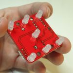
Once the through- holes have been made, you can now integrate your capacitors, transistors, LED lights, and inductors in place. Once this is done, you will have your own functional PCB in your hands. You can then proceed with your electronics project whenever you choose. Note that these basic principles also apply when designing an 8 or 16 layer PCB. All you have to do is be meticulous with your approach.
Summary
The process of designing a PCB is one that needs some practice. Therefore, with more practice comes better execution. But for many electronics enthusiasts, these processes are time-consuming and may be too technical. This is why it is advisable to simply purchase the PCB of your choice the moment you need one. It is also possible to request a PCB to be fabricated according to your own schematics. You can contact us today to learn more about how we can help.
Related posts:
 11 Programmable Robot Toys for Kids
 Electronic Project for Beginners: Fiber Light
 Electronic DIY Metal Detector Project
 Electronic DIY Project: Building Your Own Oscilloscope
 Electronic DIY Project for Your Lover
 The Different Types of Circuit Boards And What You Should Know
 Electronic Project: The Making of an Electronic Dice
 Capacitor Code And Values